
A newly synthesized form of boron has broken two expectations at once. The conductive boron material known as Imma-B60 carries electricity far better than conventional beta-boron while also tolerating about 23% plastic deformation in nanoscale compression tests. The science is striking, but the engineering question is harder: can a material made through a high-pressure precursor route become practical enough for real components?
Imma-B60 Changes the Conductive Boron Material Equation
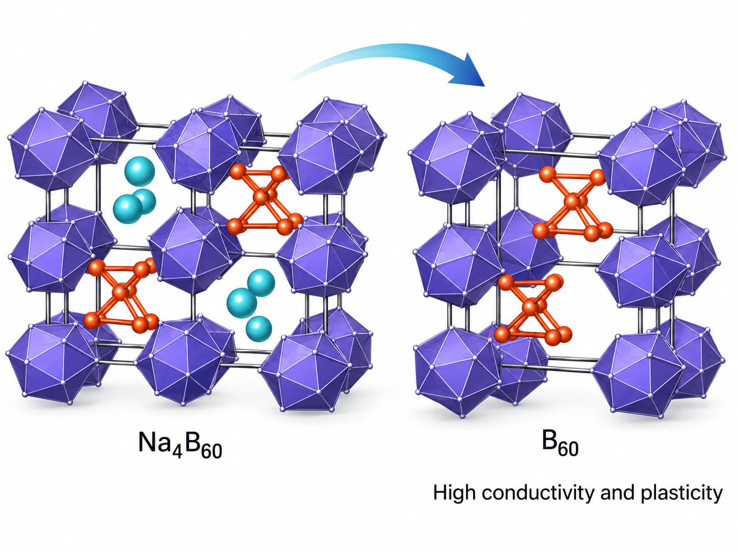
Elemental boron is usually associated with hardness, brittleness and relatively poor electrical conductivity. Imma-B60 departs from that pattern because its crystal structure is unusually open. The framework is built from B12 icosahedra linked by triangular B3 units, creating a metastable arrangement unlike familiar boron phases.
The peer-reviewed Imma-B60 study reports a bandgap below 0.2 eV and conductivity of roughly 9 × 10² S/m, about seven orders of magnitude higher than beta-boron. Those numbers do not make Imma-B60 a replacement for conventional metal conductors, but they change what engineers can plausibly ask from elemental boron.
The more significant point is the combination. Hard, strongly covalent materials often fail by brittle fracture because dislocations cannot move easily. Imma-B60 instead showed dislocation-mediated slip, suggesting its open framework can accommodate permanent shape change before failure.
Plasticity Is the Bigger Surprise
The reported 23% figure needs careful interpretation. It came from in situ uniaxial compression of nanoscale pillars, not from bending sheets, stretching wires or loading bulk components. Mechanical behavior can change with specimen size, crystal orientation, defects and processing history.
Still, the result widens the design conversation. A material that combines semiconducting electrical behavior with meaningful plastic accommodation could be interesting where brittle failure is a limiting concern. Possible long-term targets might include specialized electronic structures, sensors or components exposed to demanding mechanical conditions.
That remains a possibility, not a demonstrated application. Engineers would need evidence from larger samples, multiple orientations, repeated loading and environmental testing before treating the observed deformability as a dependable design property.

The Synthesis Route Is the Real Engineering Test
Imma-B60 was not produced by simply melting and casting boron. Researchers first formed a sodium-boron precursor, Na4B60, under high pressure. Sodium was then removed under vacuum at 900°C, leaving the open boron framework; the two-step synthesis route is central to why the phase can exist.
That precursor strategy is scientifically valuable because it can reach metastable structures that conventional equilibrium processing may not produce. It also creates an immediate manufacturing problem. High-pressure synthesis and controlled degassing are difficult to translate into large, inexpensive, repeatable production.
The gap is familiar across advanced materials. Work on materials R&D platforms shows why faster synthesis and characterization matter only when repeatability, process control and scale follow. For Imma-B60, the next challenge is proving that the structure can be made consistently enough to engineer around.
The current evidence can be separated from the unanswered manufacturing questions:
| Lab finding | What it establishes | Engineering question |
|---|---|---|
| ~9 × 10² S/m conductivity | Much higher conductivity than beta-boron | Can it persist in larger, processed parts? |
| Bandgap below 0.2 eV | Distinct electronic behavior | Can contacts and devices exploit it reliably? |
| ~23% plastic deformation | Nanopillars deform through dislocation slip | Does bulk material behave similarly? |
| High-pressure Na4B60 precursor | A removable scaffold can create the phase | Can pressure, yield and cycle time support scale-up? |
| Sodium degassing | The framework survives sodium removal | Can residual sodium and defects be controlled? |
Every compelling result is therefore paired with a scale-up question.
Electronics Potential Depends on Integration, Not Conductivity Alone
A seven-order conductivity increase sounds device-ready, but engineering decisions depend on absolute performance, stability and interfaces. Imma-B60 still conducts far less efficiently than conventional metals, so its appeal would have to come from a useful property combination rather than conductivity alone.
That could mean environments where low mass, unusual bonding or mechanical tolerance matter alongside electrical behavior. Yet those application advantages have not been validated in finished devices.
Integration would introduce contact resistance, surface chemistry, oxidation, patterning, joining, dimensional control and compatibility with existing fabrication temperatures. A material can look exceptional in isolated-property tests and still fail commercially because the process window is too narrow.
For that reason, device integration evidence will matter more than another headline number.
The Signals That Would Move Imma-B60 Toward Engineering Use
The next useful results will be less dramatic than the discovery. Researchers need larger samples, reproducible property distributions and synthesis yields across repeated batches. Scale and repeatability are the first filters.
Mechanical testing also has to move beyond nanopillars. Bulk or thin-film specimens should be tested across orientations, temperatures and loading modes, with fracture behavior characterized alongside plastic strain. Electrical measurements need similar expansion, including temperature dependence, cycling stability and the effect of defects or residual sodium.
Manufacturing researchers will also need to test whether lower-pressure routes, shorter degassing cycles or alternative precursor chemistries can preserve the framework. If the phase depends on narrowly controlled high-pressure processing, it may remain scientifically important but industrially specialized.
Cost will eventually become unavoidable. Process economics and yield often decide whether a promising material becomes a component or remains a laboratory reference point.
Imma-B60 Has Earned Attention, Not Adoption
The conductive boron material Imma-B60 changes the scientific picture of what elemental boron can do. Its high relative conductivity, narrow bandgap and unusual plastic deformation show that boron does not have to remain confined to the familiar hard-and-brittle profile.
But the decisive story now moves from discovery to manufacturing. The opportunity is a new design space for electrically active, mechanically accommodating boron structures. The pressure point is whether the high-pressure precursor route can produce useful quantities with controlled defects, repeatable properties and acceptable cost.
Until those questions are answered, Imma-B60 is best viewed as an engineering candidate, not an engineering material. That distinction defines the work required to make the discovery matter outside the laboratory.
Frequently asked questions
What is Imma-B60?
Imma-B60 is a newly synthesized boron allotrope with an open framework. It combines much higher electrical conductivity than beta-boron with unusual plastic deformation observed during nanoscale compression testing.
Is Imma-B60 actually ductile?
Not yet in the conventional engineering sense. Its roughly 23% plastic deformation was measured in nanoscale pillars under specific compression conditions. Bulk behavior, fracture resistance, orientation effects and long-term reliability still need broader testing.
What is the biggest obstacle to commercial use?
The main barrier is manufacturing. Imma-B60 currently depends on forming a sodium-boron precursor under high pressure and then removing sodium, so scale, throughput, defect control, yield and cost remain unresolved.


