
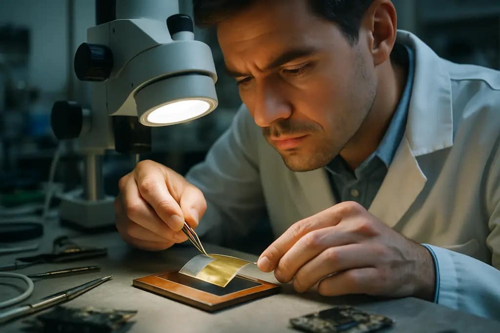
Non-Inert Substrates challenge a long-running simplification in electronic design: that the support material can be treated as mostly passive once a thin film is deposited. Research from 2025 and 2026 suggests a more cautious view. In several device classes, the substrate can store strain, affect cracking, alter adhesion behavior, influence radio-frequency loss, or change reliability under bending and humidity stress.
The implication is not that passive-substrate assumptions are always wrong. Many mature devices still perform well with established substrate stacks. The evidence does suggest that thin film performance should be interpreted as a film-substrate-system result, especially in flexible electronics, transparent conductors, silicon photonics, oxide electronics, and non-conventional photovoltaic structures.
Why Non-Inert Substrates Change Device Assumptions
Thin film design often starts with film thickness, conductivity, optical transmission, carrier behavior, thermal budget, and patterning limits. Substrate properties are usually included, but they may be simplified into surface roughness, expansion coefficient, dielectric behavior, and maximum process temperature. That approach can miss feedback from the substrate after the device begins operating.
Non-Inert Substrates And Strain Feedback
On June 18, 2026, researchers published work in Science on voltage applied to a vanadium dioxide thin film on sapphire. The reported response was not limited to the VO₂ layer. Asymmetric strain extended deeply into the Al₂O₃ substrate, reaching tens of microns, more than 200 times the thickness of the film described in the research notes. The same work indicated that strain direction imposed through the substrate fed back into the film and affected filament expansion.
This finding matters because filamentary conduction and phase-change behavior are often modeled as local film phenomena. If the substrate participates mechanically over depths far larger than the film thickness, a device designer may need to revisit assumptions about boundary conditions, repeatability, and scaling. The result is still a specific material system, not a universal rule for every oxide device. It does, however, provide evidence that substrate mechanics can become part of device operation rather than only a packaging concern.
What Counts As Device Performance
Performance is not a single number. A thin film may meet its target sheet resistance on a flat test coupon while failing after bending. A transparent electrode may pass initial optical transmission targets but drift after heat and humidity exposure. A photonic device may maintain optical behavior under repeated bending in one substrate system, while another stack cracks because the brittle layer and polymer beneath it respond differently to strain.
That is why Non-Inert Substrates require wider test plans. Electrical, optical, mechanical, and environmental measurements need to be read together. A low-resistance film that depends on an adhesion layer, a surface treatment, or a strain-relief interlayer cannot be judged only by the deposited conductor.
Flexible Devices Show The Durability Question
Flexible electronics put substrate effects under direct mechanical stress. On September 9, 2025, Brown University reported research showing that thin, brittle ceramic electrode layers could initiate cracks that propagated deeper into flexible polymer substrates. The team addressed the mismatch by adding an intermediate layer intended to reduce elastic mismatch, according to the Brown University report. The key point for engineering teams is that failure can move below the visible thin film and into the support layer.
That finding is relevant for foldable displays, flexible sensors, thin wearable components, and flexible energy devices, but it should not be treated as a finished durability recipe for all products. The reported approach points to a mechanism and a mitigation path. Product qualification would still need bending radius limits, cycle counts, humidity exposure, temperature range, chemical exposure, and manufacturing variation data for the exact stack.
Transparent And Flexible Photonics
On September 3, 2026, MIT researchers described a fabrication platform for flexible and transparent silicon photonic chips made on 300-mm wafers. The chips maintained performance after thousands of bends around cylinders as narrow as a small screw, with no noticeable optical degradation reported by MIT News in its MIT News report. That is an important laboratory-scale and wafer-scale fabrication signal, especially because silicon photonics usually depends on precise optical confinement and low-loss structures.
The result does not prove immediate readiness for every consumer, medical, aerospace, or industrial application. It does show that substrate engineering can open design options that rigid wafers do not allow. Qualification would still need stress aging, contamination control, bonding and packaging studies, thermal cycling, connector strategy, and yield data across the process flow.
Conductive Films Under Bending And Humidity
Other 2026 research noted in the supplied materials reported transparent conductive electrode structures on PET that combined Cu/NiCr interfacial layers with high adhesion ratings, around 10.8 ohms per square sheet resistance, more than 87 percent transmittance at 550 nm, and less than 5 percent sheet resistance change after 1,000 bending cycles. The same notes described operation for more than 20 hours under damp heat at 85 °C and 85 percent relative humidity.
Those figures are useful because they combine optical, electrical, adhesion, bending, and humidity data. They remain early evidence unless matched to a defined product duty cycle. For manufacturing, the unresolved questions include film uniformity over large areas, cost of interfacial layers, compatibility with roll-to-roll processing, and long-duration field exposure.
Manufacturing Questions For Non-Inert Substrates
Non-Inert Substrates affect process development because the substrate is part of the deposition and reliability problem. A stack that works on a polished research substrate may not transfer cleanly to paper, textile, elastomer, ceramic, metal foil, or polymer without changes in nucleation, continuity, stress, and thermal handling.
The 2026 research notes on non-conventional photovoltaic substrates identified practical barriers: porosity, surface roughness, thermal transport limits, and outgassing can degrade nucleation, film continuity, and device reliability. Those points fit a broader pattern in thin film scale-up, where strong lab data must be checked against stability, yield, supply risk, and field evidence. A related discussion of thin-film materials for clean energy covers similar scale questions in energy applications, and related energy-sector materials coverage can be explored through Illinois Energy resources.
Process Trade-Offs Are Material-Specific
The supplied research notes also described RF components on high-resistivity silicon where silicon nitride films deposited by different methods produced sharply different surface conductivity values. Physical vapor deposition SiₓNᵧ layers were reported near 2 S/m, while plasma-enhanced chemical vapor deposition layers were reported near 450 S/m because of hydrogen-related effects, with insertion loss affected as a result. The lesson is not that one deposition method is always superior. It is that deposition chemistry, substrate choice, and frequency regime can interact in ways that are invisible if the substrate is treated as an inert carrier.
Commercial substrate announcements also show that suppliers are pushing material properties toward high-frequency use. In December 2025, Murata announced an inner-cavity liquid crystal polymer flexible substrate with dielectric constant below 2.0, aimed at 7 GHz to 24 GHz operation. Supplier data can guide early screening, but design teams still need independent validation under their stack geometry, copper thickness, adhesive system, and assembly process.
| Design Area | Substrate-Related Risk | Evidence To Request |
|---|---|---|
| Mechanical reliability | Crack initiation or propagation into polymer supports | Bending radius, cycle count, crack imaging, post-test resistance |
| Oxide electronics | Strain feedback from substrate into active film | In-operando strain mapping and device-state correlation |
| Transparent conductors | Adhesion loss, oxidation, humidity drift | Sheet resistance, transmittance, damp-heat aging, peel or tape tests |
| RF substrates | Loss changes from dielectric chemistry or surface conduction | Insertion loss, dielectric data, deposition history, hydrogen content indicators |
| Photonic chips | Optical degradation after bending or packaging | Loss measurements before and after bending, thermal cycling, assembly tests |
Cost and safety also deserve early attention. Some interlayers or overlayers add process steps. Some polymers limit process temperature. Some metal or ceramic surfaces need cleaning steps that may affect worker exposure controls or waste handling. These are not reasons to reject an approach, but they are reasons to include process engineers, reliability teams, and environmental health and safety staff before a stack is locked.
Non-Inert Substrates in Electronic Design Practice
The practical shift is to qualify the stack, not just the film. Non-Inert Substrates should be part of the device model, the test coupon design, and the failure-analysis plan. If a film changes strain state during operation, if a polymer substrate cracks below a brittle electrode, or if a dielectric deposition route changes RF loss, the substrate is part of the active engineering problem.
Evidence-Based Design Rules
Design teams can respond without assuming that every new substrate study is ready for production. A sound approach is to define the mechanism being claimed, identify the test conditions, compare them with the intended duty cycle, and require repeatable measurements on the actual material stack. For early-stage research, the right question is not whether it has solved a production problem. The right question is what risk it identifies, what design variable it changes, and what data would be needed before adoption.
For thin film electronics, the evidence from 2025 and 2026 points to a more integrated design discipline. Substrates can influence strain, cracking, optical stability, RF loss, and environmental durability. Treating them as active participants will not remove the need for cost control, yield learning, and long-term reliability work. It will, however, make thin film device evaluation closer to how these materials behave in service.


