
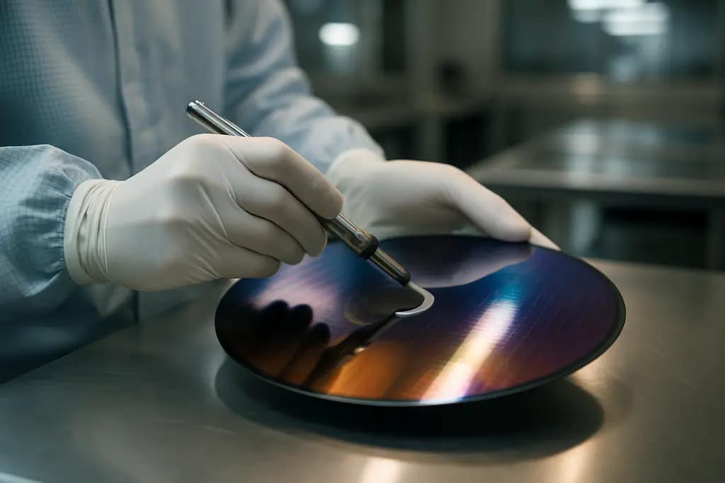
thin-film semiconductor coatings are drawing attention because recent Princeton work has shown unusual control over ultrathin semiconductor behavior, but the evidence still points to an early-stage manufacturing problem rather than a ready product platform. The central product-design issue is not whether a lab sample can show useful electronic or optical properties. It is whether those properties can be reproduced across larger areas, processed through standard steps, and kept stable under operating conditions.
For manufacturers, the distinction matters. A coating that works on a small sample may fail to meet cost, yield, inspection, or reliability targets once it is moved toward wafer-scale processing or fielded devices. Recent Princeton studies help define where the technical promise sits today: promising at the materials-science level, but constrained by uniformity, interfaces, contamination, and integration requirements.
Where thin-film semiconductor coatings Stand
Why thin-film semiconductor coatings Are Still Early
The research base described here should be read as laboratory and process-development evidence, not as proof of a commercial coating route. For thin-film semiconductor coatings, the strongest signals from the Princeton-related work are about controllability and processing direction. They do not remove the need for qualification across larger substrates, repeat runs, long-duration exposure, and complete device stacks.
A 2026 Princeton report described work led by Saien Xie on an ultrathin, photo-programmable semiconductor only a few molecules thick. The researchers produced a uniform one-inch-square sample with reprogrammable electronic and optical properties, according to the Princeton Materials release. That scale is meaningful for demonstrating material behavior, yet it is still far from the area, repeatability, and defect tolerance expected in many production environments.
The Princeton Photo-Programmable Result
The photo-programmable result is relevant to product design because it suggests a route for changing semiconductor properties after fabrication. In a design review, that possibility would raise practical questions. How repeatable is the programming step across the full surface? Does the change remain stable after thermal cycling, light exposure, packaging stress, or electrical operation? Can the process be inspected without damaging the active layer?
The reported one-inch-square uniform sample is therefore best viewed as a controlled research milestone. It does not mean that thin-film semiconductor coatings can be specified today as a drop-in production coating for sensors, displays, computing components, or energy devices. The gap between a sample and a qualified product includes substrate compatibility, deposition control, patterning, encapsulation, yield analysis, and accelerated aging data.
Wafer-Scale Uniformity Is The First Design Constraint
From One-Inch Samples To Wafers
Scaling thin-film semiconductor coatings from small samples to wafers or large panels changes the engineering problem. A coating can look uniform over a limited field of view while still having thickness variation, grain boundaries, wrinkles, vacancies, contamination, or contact variation that become decisive at product scale. Product teams need to define acceptable variation early, because the inspection requirement can become as influential as the coating chemistry.
Princeton’s Alice Kunin initiated a DOE-funded project that was announced on March 13, 2025, to develop a processing toolbox for two-dimensional transition metal dichalcogenide semiconductors that could be made into homogeneous wafer-scale size and then undergo standard semiconductor processing, according to the Princeton faculty announcement. The way that goal is framed is significant: wafer-scale homogeneity is not treated as a solved detail, but as a central research objective.
Interfaces And Process Drift
At larger scale, the coating is only one part of the system. Interfaces with electrodes, substrates, barrier layers, and packaging materials can change electrical behavior or create failure sites. Small differences in deposition conditions may affect adhesion, crystallinity, carrier transport, or optical response. A product design that assumes the active film alone defines performance would miss much of the risk.
This is where the findings connect with broader scale-up concerns in thin-film materials. A related analysis of thin-film scale-up risks notes that stability, yield, supply factors, and field evidence all shape whether strong lab results can support deployment. The same caution applies here: coating performance has to survive the full production sequence, not just the first measurement.
Reliability, Contamination, And Product Qualification
Lithography And Handling Risks
Recent Princeton-related research notes also point to lithography and handling as sources of variation. Solvents, resist residues, transfer steps, and electrode formation can all affect monolayer semiconductor behavior. If a coating must pass through conventional patterning, cleaning, and metallization steps, each step becomes a possible source of contamination or damage. That does not make the material unsuitable. It means product qualification must include the process route, not only the film recipe.
For design engineers, this changes the acceptance criteria. A data sheet for a future coating would need more than mobility, optical response, or switching behavior from a small test structure. It would need lot-to-lot process controls, defect maps, interface specifications, storage limits, rework rules, and packaging constraints. Without those controls, a promising material can create unpredictable downstream yield losses.
Energy And Industrial Use Cases
Energy and industrial systems may add further exposure demands. Coatings used in power, sensing, or conversion devices may face temperature swings, humidity, vibration, ultraviolet exposure, electrical stress, or long service intervals. As readers follow developments in how materials research links to energy applications, the insights provided by Illinois Energy add related context within the same network. The practical question for any energy-linked product is whether the coating can deliver stable performance after packaging, installation, and operation, not only whether it performs well at the point of fabrication.
Cost, Safety, And Manufacturing Readiness

Inspection Adds To The Design Brief
Cost is not established by the Princeton findings alone. The studies show research direction and sample-level capability, but they do not provide a full cost model for high-volume coating, inspection, rework, or yield loss. In practice, costs would depend on substrate size, deposition throughput, material utilization, cleanroom requirements, patterning steps, metrology, and scrap rates. If uniformity is hard to maintain, inspection and yield management may become major cost drivers.
Manufacturing readiness also depends on feedback control. Thin films often require in-line or near-line measurement to track thickness, crystallinity, defects, and electrical response. If the only reliable verification method is slow, destructive, or limited to small areas, the process may be difficult to scale even when the material physics is sound. Product teams should treat metrology as part of the design architecture rather than a final quality check.
What Product Teams Can Specify Now
Even at an early stage, product teams can define requirements that make later decisions clearer. Useful specifications include target substrate size, allowed nonuniformity, interface materials, maximum thermal budget, acceptable contamination limits, expected operating environment, and test methods for programmed or reprogrammed states. These requirements help separate a promising laboratory effect from a manufacturable coating stack.
- Define whether the coating must be wafer-compatible, panel-compatible, or limited to small-area devices.
- Specify the electrical, optical, and mechanical properties that must remain stable after processing.
- Require interface and packaging tests, not only bare-film measurements.
- Identify inspection methods that can operate at the intended production scale.
Safety also belongs in this discussion. The available research does not establish a general product-safety profile. Processes involving deposition, plasma steps, solvents, lasers, or light exposure would need standard industrial hazard review, emissions controls, operator training, and waste handling appropriate to the actual process chemistry and equipment. No lab finding should be treated as a substitute for that review.
Product Design Implications For thin-film semiconductor coatings
Practical Reading Of The Princeton Evidence
The strongest product-design lesson from the Princeton studies is that scale is a performance variable. The photo-programmable semiconductor work showed controlled behavior on a one-inch-square sample, while the wafer-scale semiconductor project framed homogeneity as a research target. Taken together, those facts suggest real scientific progress, but they also mark the boundary of what has been demonstrated.
For product design teams, thin-film semiconductor coatings should be evaluated through a staged evidence model. First, confirm the material effect on small samples. Next, test whether the coating remains uniform over the intended substrate size. Then qualify interfaces, patterning, contacts, packaging, and environmental exposure. Only after those steps can cost and yield claims be assessed with confidence.
The implication is cautious but constructive. Princeton’s recent work helps clarify which questions manufacturers should ask before designing around these materials: Can the active film be made homogeneous at scale? Can it survive standard processing? Can programmed behavior be verified after packaging? Can inspection detect the defects that matter? Until those answers are supported by larger-area and longer-duration evidence, product teams should treat the technology as promising research with unresolved manufacturing constraints.


